GALs by Example, Part 3
In part two we learned how to use tri-state outputs to control access to and from a shared data bus. In this post we will learn how to implement sequential logic by using the GAL16V8 in registered mode.

GAL16V8 in Registered Mode
In registered mode we again have 16 inputs and 8 outputs, but the outputs can now be registered, meaning they do not output their values immediately, but rather latch these values on the rising edge of the clock (dedicated pin 1). All registered outputs share a single output-enable (dedicated pin 11). Here is the pinout in registered mode.
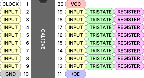
At first glance it might appear that this mode is strictly better than complex mode, as tri-state outputs are still allowed in this mode (and none have the “no feedback” restriction). The catch is that while you can indeed have eight tri-state outputs in this mode, this would leave you with only eight inputs due to pins 1 and 11 being dedicated to CLK and /OE. In complex mode you would have ten inputs available. However as far as I can tell, GALasm will only select registered mode if there is at least one registered output, so this question may be academic.
A Parallel-Load Shift Register
A common task in electronics is turning serial data into a paralle data, which we do via a shift register. We will implement a 4-bit shift register with parallel load using a GAL16V8 in registered mode.
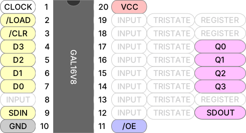
Bits shift in via SDIN on the rising edge of CLK, through bits Q0, Q1, Q2, Q3. SDOUT is identical to Q3. If /LOAD is asserted then the values on D[0:4] are copied to Q[0:4] on the rising clock. If /CLR is asserted then all bits are cleared on the rising clock.
Here is the GALasm source in its entirety.
GAL16V8
SHIFT

CLK /LOAD /CLR D3 D2 D1 D0 NC SDIN GND
/OE SDOUT  NC  Q3 Q2 Q1 Q0 NC NC   VCC

Q0.R    = /CLR &  LOAD & D0
        # /CLR & /LOAD & SDIN

Q1.R    = /CLR &  LOAD & D1
        # /CLR & /LOAD & Q0

Q2.R    = /CLR &  LOAD & D2
        # /CLR & /LOAD & Q1

Q3.R    = /CLR &  LOAD & D3
        # /CLR & /LOAD & Q2

SDOUT.R = /CLR &  LOAD & D3
        # /CLR & /LOAD & Q2

DESCRIPTION
A 4-bit parallel load shift register.
Note the following:
- We must specify
CLKat pin 1 and/OEat pin 11. These are keyword labels likeVCCandGND. - Registered outputs have the
.Rsuffix. The value is latched on the risingCLK. - Much like tri-state outputs, we refer to the feedback from registered outputs without a suffix. These refer to current latched values, which we use to compute the next latched values.
Testing
Here is a test suite for the shift register. Note the use of the C token for pin 1. This instructs minipro to issue a positive-going clock pulse before checking the output bits. Agan, refer to the post on testing GALs for more information.
<?xml version="1.0" encoding="utf-8"?>
<logicic>
  <database type="LOGIC">
    <custom name="whatever-you-want">
      <ic name="shift" type="5" voltage="5V" pins="20">

          <vector> C 01 1011 X X G 0 H X HLHH XXV </vector> <!-- Load -->
          <vector> X XX XXXX X X G 1 Z X ZZZZ XXV </vector> <!-- Disable -->
          <vector> X XX XXXX X X G 0 H X HLHH XXV </vector> <!-- Enable -->
          <vector> C 11 XXXX X 0 G 0 L X LHHL XXV </vector> <!-- Shift a 0 -->
          <vector> C 11 XXXX X 1 G 0 H X HHLH XXV </vector> <!-- Shift a 1 -->
          <vector> C 11 XXXX X 1 G 0 H X HLHH XXV </vector> <!-- Shift a 1 -->
          <vector> C X0 XXXX X X G 0 L X LLLL XXV </vector> <!-- Clear -->

        </ic>
    </custom>
  </database>
</logicic>
Exercises
- Program two shift registers and chain them together through
SDOUTandSDINto create an 8-bit shift register. - Write a 4-bit counter.